Research Projects
Hybrid inorganic/organic system
 Much attention has been spent on the utilization of materials featuring
a complexity on the nanoscale, to realize novel electronic devices or computing
architectures. Synthetic inorganic chemistry can be harnessed toward the self-assembly
of large, periodic arrays of sites with active transport properties. Such properties
can consist of current rectification, magneto-electronic phenomena usable for memory
applications, or transistor characteristics. Zeolitic materials, characterized by the
presence of nanoscale channels and cavities within their structure, occur naturally and
can also be synthesized by inorganic methods in the laboratory. The channels and cavities
occur on a periodic lattice with tunable periodicity of 0.5 to > 10 nm.
The aim of this project is to exploit nanoscale self-assembly to synthesize zeotype
crystals with potential electronic properties. Central among these electronic properties
stand quantum dot and single-electron-transistor effects obtained in the nanoscale cavities
afforded by the zeotype crystals. One crystal contains millions to billions of cavities,
and hence an equal number of identical electronic devices. We propose addressing of
individual devices by, for example, DNA segments. DNA offers the advantage that it can
be flexibly functionalized with end groups with affinity for either the metallic external
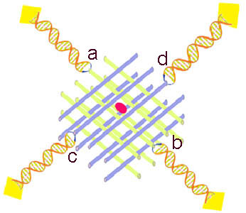
electrodes or the zeolitic materials chain ends. The sketch depicts a zeotype crystal,
with DNA chains providing electrical leads connected to crystal face sites a to d, and to
lithographically defined gold contact pads. The red elliptical area depicts a
single-electron-transistor (SET) site, dominating conduction between contacts a and b and
tuned by voltages applied to contacts c and d. This approach not only provides large
numbers of individual devices, but an interconnecting architecture as well, provided by
the zeotype framework. Such self-assembled and chemically contacted arrays of single-electron
transistors show promise as computational hardware or as memory devices. This concept is
the basis of an NSF NIRT grant Zeolitic materials for nanoscale electronics and quantum computation.

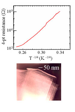
Hydro- and solvo-thermal routes are utilized for the
synthesis of novel zeolitic materials with desired functionalities.
These approaches have yielded, in addition to other materials, a
series of vanadium based nanowires, VOx (organic)y [where x is
between 3 and 3.5 and y is between 0.1 and 0.5], with diverse
electronic properties, from band insulator to hopping conductor.
These nanotubes and scrolls house organic cations, and it appears
that the ratio of organic molecules to the VO3 unit influences the
electronic properties. On the top left is a resistance versus
temperature plot of a bundle of one of these nanowires that exhibits
Mott variable range hopping conductivity. The bottom left TEM image depicts
the scroll nature of some of the nanowires.

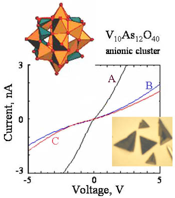
Another vanadium system exhibiting DC electrical conduction
is found in a compound consisting of anionic V10As12O40 clusters connected
via organic cations and water molecules. Pyramidal shaped, dark brown
single crystals of the compound were isolated via hydrothermal synthesis,
and the lower insert in the figure on the right depicts an optical image of
some of these crystal alongside a needle tip (diameter 0.83 mm) for size
comparison. The upper insert depicts a polyhedral model of the cluster,
obtained from single crystal X-ray studies. The I-V plot represents 3
curves for 3 samples from different reactions. Curves B and C were
obtained with contacts along similar crystal orientation, whereas for
curve A, the contacts were along an orientation roughly perpendicular
to those used for curves B and C.
 Much attention has been spent on the utilization of materials featuring
a complexity on the nanoscale, to realize novel electronic devices or computing
architectures. Synthetic inorganic chemistry can be harnessed toward the self-assembly
of large, periodic arrays of sites with active transport properties. Such properties
can consist of current rectification, magneto-electronic phenomena usable for memory
applications, or transistor characteristics. Zeolitic materials, characterized by the
presence of nanoscale channels and cavities within their structure, occur naturally and
can also be synthesized by inorganic methods in the laboratory. The channels and cavities
occur on a periodic lattice with tunable periodicity of 0.5 to > 10 nm.
The aim of this project is to exploit nanoscale self-assembly to synthesize zeotype
crystals with potential electronic properties. Central among these electronic properties
stand quantum dot and single-electron-transistor effects obtained in the nanoscale cavities
afforded by the zeotype crystals. One crystal contains millions to billions of cavities,
and hence an equal number of identical electronic devices. We propose addressing of
individual devices by, for example, DNA segments. DNA offers the advantage that it can
be flexibly functionalized with end groups with affinity for either the metallic external
electrodes or the zeolitic materials chain ends. The sketch depicts a zeotype crystal,
with DNA chains providing electrical leads connected to crystal face sites a to d, and to
lithographically defined gold contact pads. The red elliptical area depicts a
single-electron-transistor (SET) site, dominating conduction between contacts a and b and
tuned by voltages applied to contacts c and d. This approach not only provides large
numbers of individual devices, but an interconnecting architecture as well, provided by
the zeotype framework. Such self-assembled and chemically contacted arrays of single-electron
transistors show promise as computational hardware or as memory devices. This concept is
the basis of an NSF NIRT grant Zeolitic materials for nanoscale electronics and quantum computation.
