Organic semiconductors
Another area of molecular electronics pursued is organic semiconductors,
systems that exhibit conjugation and/or pi-to-pi interactions. Already, LEDs fabricated
from organic semiconductors are utilized for displays (see for example Scientific American,
February 2004). Worldwide, both academic and industrial research on thin film organic Field-Effect
Transistors (OFETs) aims at investigating this alternative to traditional semiconducting devices
for a variety of applications. For organic semiconductors,
usually p-type behavior is observed, either due to easier
hole injection or due to doping (e.g. oxygen) or defects.
Yet, both n- and p-type behavior are necessary for the
implementation of Complementary Metal Oxide Semiconductor (CMOS) technology. [J. Jo et al.
Gate tunable electron injection in submicron pentacene transistors Nanotechnology 15, 1023 (2004)].
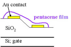
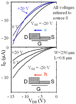
To realize ambipolar behavior for organic thin films, we utilize a novel device geometry that
allows for the observation of both hole and electron currents in pentacene OFETs, due to the
symmetric electric fields at the contacts. As seen in the current-voltage characteristics,
when the lower contact is the drain, there is a cross-over point where we observe n-type behavior.
When the upper contact functions as the drain, we observe p-type behavior. The higher electric
field at the lower contact compensates for the 1.35 eV injection barrier for electrons from gold
into pentacene, while the submicron channel length allows for the short electron lifetimes in pentacene.
Although the demonstration of this ambipolar charge transport was realized for a pentacene OFET on
SiO2/Si substrate, the fabrication process may be used for a variety of substrates and for other
organic materials as well.
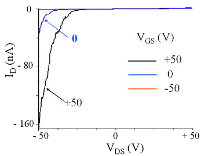
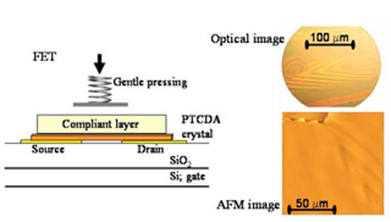
PTCDA (3,4,9,10-perylenetetracarboxylic dianhydride) is another organic material
under investigation. Compared to pentacene, the LUMO level of PTCDA is closer to the workfunction
of gold. Field-effect transistors of single crystal PTCDA were fabricated with a bottom contact
geometry (L = 15 micron, W = 2 mm). The crystals were placed on the device and gently pressed to
ensure contact. The FET structures were realized by placing the smooth side of crystal
on the contacts. The ensuing transfer characteristics indicate the expected n-type behavior.
Interestingly, when the device is exposed to atmospheric conditions, the electron current
diminishes, until, after 20 days, one only measures a few nA.